- $2.4B → $5.9Bprojected growth in laser and photonic integrated circuit sales for optical transceivers, 2023 to 2029, driven largely by AI data centers
- 2025the year deployment-ready CPO products first arrived commercially
- 51.2 Tbpsthroughput of Broadcom’s CPO switch platform, delivered in 2024 as an early commercial proof point
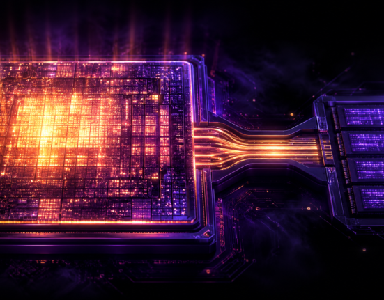
Every AI cluster scaling past a handful of racks runs into the same physical limit: copper electrical interconnects lose signal integrity and burn power at a rate that gets worse, not better, as bandwidth demand rises. Co-packaged optics (CPO) is the industry’s answer — integrating photonic integrated circuits and lasers directly alongside the switching ASIC or processor inside the same package, rather than routing electrical signals out to a separate optical transceiver module at the edge of a server. Shortening that electrical path is the entire point: it’s where most of the power loss and signal degradation actually happens.
Why this matters specifically for AI clusters, not general networking
General enterprise networking has used optical transceivers for years without needing co-packaging, because the bandwidth and density demands were modest enough that a modular pluggable optic at the edge of a switch was good enough. AI training and inference clusters broke that assumption: thousands of accelerators need to exchange enormous volumes of data at extremely low latency, and every additional watt spent moving that data instead of computing on it is a direct tax on the cluster’s useful output. CPO addresses this bandwidth and latency bottleneck directly, shortening the high-speed electrical path and enabling denser, lower-power optical fabrics — which is why the shift is being driven specifically by AI inference and training demand rather than general data center growth.
| Pluggable optical transceiver | Co-packaged optics | |
|---|---|---|
| Optics location | Separate module at the edge of the switch or server | Integrated directly alongside the switching ASIC or processor die |
| Electrical path length | Longer — signal travels from die to edge before conversion | Short — conversion happens right next to the die |
| Power per bit | Higher, due to longer electrical signal travel | Lower — the core value proposition of CPO |
| Market status in 2026 | Mature, widely deployed | Deployment-ready as of 2025, scaling through 2026 |
Where the technology actually stands right now
Deployment-ready CPO products only arrived in 2025, which makes 2026 the first year this is a real production decision rather than a roadmap slide. Broadcom delivered a 51.2 Tbps CPO switch platform in 2024 as an early proof point, and NVIDIA has moved to implement silicon photonics and co-packaged optics for AI GPU communication specifically for its 2026 generation, positioning the technology as increasingly mandatory rather than optional for next-generation AI data centers. The laser and photonic integrated circuit market feeding this transition is projected to grow from $2.4 billion in 2023 to $5.9 billion by 2029, with AI data centers cited as the primary driver of that growth.
- 1. Bandwidth demand outpaces copperThousands of accelerators exchanging data at extreme volume make copper’s power and signal-integrity limits binding.
- 2. Optics move toward the diePhotonic integrated circuits and lasers are packaged directly alongside the switching ASIC or processor.
- 3. Electrical path shrinksShorter high-speed electrical runs cut power per bit and improve signal integrity where it matters most.
- 4. Vendor roadmaps convergeNVIDIA’s 2026 GPU communication roadmap and Broadcom’s shipped CPO switch platform both point toward optics displacing copper at the highest-bandwidth links.
Why CPO moved from research topic to deployment decision in 2026
Aggressive vendor roadmaps suggest optics eventually take over all high-bandwidth interconnects — but that transition is happening link by link, not all at once.
What CPO does not solve — and where the real limit still is
CPO addresses interconnect power and bandwidth density; it does not touch the compute or memory bottlenecks covered elsewhere in this cluster. A cluster with excellent optical interconnects is still capped by HBM bandwidth for memory-bound inference workloads, and still competing for the same constrained CoWoS packaging capacity used to bond compute dies to memory in the first place. CPO is a genuine, necessary improvement to one specific layer of the stack — it is not a solution to the AI infrastructure supply crunch as a whole, and vendors positioning it that way are overselling its scope.
Adopt CPO for new high-bandwidth cluster links Increasingly standard
Right for new AI cluster builds where interconnect power and density are binding constraints — this is where major vendor roadmaps are converging for 2026 and beyond.
Continue with pluggable optics for moderate-scale deployments Still viable
Reasonable for clusters where interconnect bandwidth isn’t yet the binding constraint, avoiding the integration complexity and cost premium of first-generation CPO products.
Expect CPO to resolve broader AI compute or memory bottlenecks Wrong expectation
CPO improves interconnects specifically; it does nothing for HBM memory bandwidth or CoWoS packaging capacity constraints elsewhere in the same cluster.
Common mistakes
Common mistake
Treating “co-packaged optics” and “optical computing” as the same trend. CPO is an interconnect technology moving optics closer to the die; it does not perform computation optically the way true photonic processors aim to — conflating the two overstates what CPO actually delivers.
Common mistake
Assuming CPO adoption alone resolves an AI cluster’s throughput problems. Interconnect improvements matter, but a cluster still bottlenecked on HBM bandwidth or GPU allocation won’t see proportional gains from optics alone.
What worked
Teams planning new large-scale AI clusters treated CPO adoption as one line item in a broader interconnect and power budget, evaluating it specifically against measured power-per-bit and density requirements for their planned scale, rather than adopting it reflexively because major vendors were promoting it.
Glossary
- Co-packaged optics (CPO)
- An interconnect architecture that integrates photonic components directly alongside a switching ASIC or processor within the same package, shortening the electrical signal path.
- Photonic integrated circuit (PIC)
- A chip that processes optical signals using integrated photonic components, analogous to how an electronic integrated circuit processes electrical signals.
- Pluggable optical transceiver
- A separate optical module located at the edge of a switch or server, the conventional alternative to co-packaged optics.
- Power per bit
- A measure of energy consumed per unit of data transmitted — the primary metric CPO is designed to improve over conventional electrical and pluggable-optical interconnects.
Key takeaways
- Co-packaged optics integrates photonic components directly alongside a switching ASIC or processor, shortening the electrical path and reducing power per bit compared to edge-mounted pluggable transceivers.
- Deployment-ready CPO products only arrived commercially in 2025, making 2026 the first year this is a genuine production decision for AI cluster builders rather than a research roadmap item.
- NVIDIA has moved to implement silicon photonics and co-packaged optics for GPU-to-GPU communication in its 2026 generation, signaling the technology is becoming close to mandatory for next-generation AI clusters.
- The laser and photonic integrated circuit market feeding optical transceivers is projected to grow from $2.4 billion in 2023 to $5.9 billion by 2029, driven largely by AI data center demand.
- Broadcom’s 51.2 Tbps CPO switch platform, delivered in 2024, was an early commercial proof point that helped establish CPO as production-viable rather than experimental.
- CPO solves an interconnect power and bandwidth problem specifically — it does not resolve separate HBM memory bandwidth or CoWoS packaging capacity constraints elsewhere in an AI cluster’s stack.
- The most effective adoption approach evaluates CPO against measured power-per-bit and bandwidth density needs for a specific planned cluster scale, rather than adopting it simply because major vendors are promoting it.
FAQs
What is co-packaged optics and how is it different from a regular optical transceiver?
Co-packaged optics integrates photonic components and lasers directly alongside a switching ASIC or processor within the same package, shortening the electrical signal path, whereas a conventional pluggable optical transceiver sits as a separate module at the edge of a switch or server.
Why does AI specifically need co-packaged optics more than general networking?
Because AI training and inference clusters move enormous volumes of data between thousands of accelerators at extremely low latency, making the power and signal-integrity costs of longer electrical paths a direct tax on useful compute output in a way general enterprise networking rarely experiences.
Is co-packaged optics actually deployed yet, or still experimental?
It became deployment-ready in 2025, and 2026 is the first year it represents a genuine production decision for AI cluster builders — Broadcom shipped a 51.2 Tbps CPO switch platform as an early commercial proof point in 2024.
Is NVIDIA adopting co-packaged optics?
Yes. NVIDIA has moved to implement silicon photonics and co-packaged optics for GPU communication specifically in its 2026 generation, positioning the technology as increasingly mandatory for next-generation AI data centers.
Does co-packaged optics solve AI infrastructure’s other supply bottlenecks?
No. CPO addresses interconnect power and bandwidth specifically — it does not resolve separate constraints like HBM memory bandwidth or TSMC’s CoWoS advanced packaging capacity, both of which remain binding regardless of interconnect improvements.
How big is the market driving co-packaged optics adoption?
The laser and photonic integrated circuit market for optical transceivers is projected to grow from $2.4 billion in 2023 to $5.9 billion by 2029, with AI data centers cited as the primary driver of that growth.
Is co-packaged optics the same as photonic computing?
No. Co-packaged optics is an interconnect technology that moves data between chips using light; photonic computing aims to perform the actual computation optically, a distinct and less mature technology covered separately.
Should every new AI cluster adopt co-packaged optics immediately?
Not necessarily. It’s most valuable where interconnect power and bandwidth density are the binding constraint; smaller or moderate-scale deployments may reasonably continue with pluggable optics until that constraint becomes real for their specific scale.
References
- SemiAnalysis — “Co Packaged Optics (CPO) – Scaling with Light for the Next Wave of Interconnect”
- Siemens — “Five Key Trends of Co-Packaged Optics (CPO) in 2026”
- EDN — “Where co-packaged optics (CPO) technology stands in 2026”
- IndexBox — “OFC 2026: Optical Interconnects Dominate AI Data Center Future”
Related reading on The Tech Trends: HBM Memory Bandwidth, Advanced Packaging, GPU Shortage Economics, and Photonic Computing for AI.