- 35,000 → 130,000TSMC’s CoWoS wafer-per-month capacity, late 2024 to projected end of 2026
- >50%share of TSMC’s 2026-2027 CoWoS capacity reportedly already booked by NVIDIA alone
- $1,000-1,100reported cost of CoWoS-L packaging for NVIDIA’s B200, a 47% premium over simpler packaging driven by multi-die complexity
For years, the AI chip conversation focused on fab capacity — how many wafers TSMC’s most advanced process nodes could produce. That’s no longer where the constraint sits. The actual bottleneck preventing hyperscalers from deploying AI capacity as fast as they’d like is advanced packaging: the process of bonding a finished logic die together with high-bandwidth memory dies onto a single substrate, which modern AI accelerators require because no single die can economically contain both the compute logic and the memory bandwidth a GPU needs.
What advanced packaging actually does, and why it’s necessary
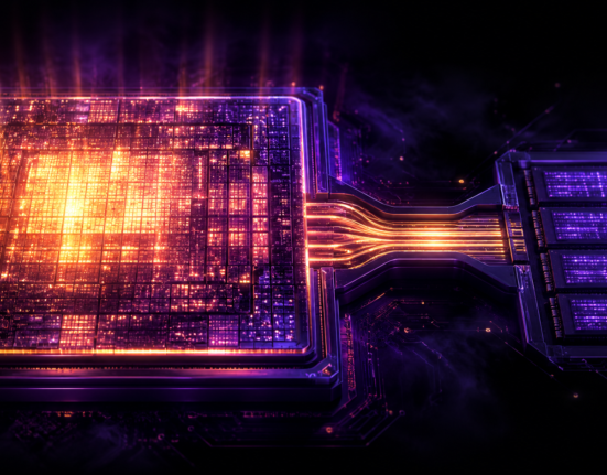
TSMC’s Chip on Wafer on Substrate (CoWoS) process is the specific technology at the center of this constraint. It’s a 2.5D and 3D packaging approach that connects high-performance logic chips with high-bandwidth memory by bonding multiple dies onto an interposer and substrate with extremely fine, precise interconnects. This isn’t optional cosmetic packaging — it’s the physical mechanism that makes it possible to place HBM stacks close enough to a GPU die to deliver the bandwidth modern AI workloads need. Without advanced packaging, a manufactured GPU die and manufactured HBM stacks would simply be two separate, unconnected pieces of silicon.
| Fab capacity (wafer production) | Advanced packaging capacity (CoWoS) | |
|---|---|---|
| What it produces | The raw logic die and memory dies themselves | The bonded, connected assembly combining logic and memory into a working accelerator |
| 2026 constraint status | Real, but less binding than packaging | The primary bottleneck on total finished accelerator output |
| Expansion timeline | Multi-year, new fab construction | Faster to expand than a new fab, but still heavily allocated through 2026 |
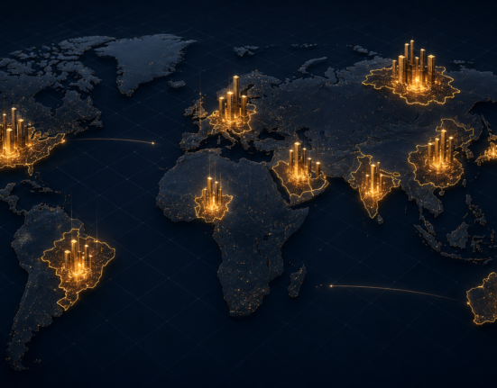
| Geographic concentration | Concentrated in a few advanced-node fabs globally | Taiwan ~45% of Q1 2026 capacity, South Korea ~20%, China ~15% |
Why NVIDIA’s booking dominance matters for everyone else
NVIDIA has reportedly booked over half of TSMC’s total CoWoS capacity for 2026-2027, which underscores both the immense demand for its GPUs and just how little capacity is left over for competitors, custom silicon builders, and any other player needing advanced packaging for their own AI accelerator designs. This is a structurally different kind of scarcity than a general shortage — it’s a specific company’s forward bookings crowding out the available slots on a specific, hard-to-expand manufacturing process, meaning a competitor with sufficient capital still can’t simply buy its way into more packaging capacity if the slots are already contractually committed elsewhere.
- 1. Logic and memory manufactured separatelyGPU compute dies and HBM memory stacks are fabricated independently, at their own respective fabs.
- 2. CoWoS bonds them togetherTSMC’s advanced packaging process connects logic and memory dies onto a shared substrate with precise interconnects.
- 3. Capacity gets booked years aheadNVIDIA reportedly secures over half of 2026-2027 CoWoS capacity, leaving a shrinking remainder for everyone else.
- 4. TSMC scales aggressively, but demand outpaces itCoWoS capacity nearly quadruples from 35,000 to a projected 130,000 wafers per month, yet remains heavily allocated throughout 2026.
Why packaging, not the fab, is the actual output ceiling on AI accelerators
Even TSMC’s aggressive capacity expansion — nearly quadrupling output in about two years — hasn’t been enough to fully relieve the constraint given how fast demand has grown alongside it.
The cost premium of chiplet complexity
Advanced packaging isn’t just capacity-constrained; it’s also meaningfully more expensive per unit than simpler packaging approaches, and that cost scales with complexity. CoWoS-L packaging for NVIDIA’s B200 reportedly costs $1,000 to $1,100 per unit, a 47% premium specifically attributable to the multi-die complexity involved in bonding multiple chiplets and HBM stacks together precisely. That premium is a real, measurable tax on every advanced AI accelerator built this way, on top of whatever capacity allocation constraint a given buyer faces — meaning packaging economics affect the cost structure of AI hardware even for buyers who do manage to secure capacity.
Secure multi-year packaging capacity commitments early What NVIDIA did
Booking capacity years in advance, as NVIDIA has reportedly done for 2026-2027, is the only reliable way to guarantee advanced packaging access in a supply-constrained environment.
Diversify across packaging providers and geographies Emerging strategy
With capacity concentrated roughly 45% in Taiwan, 20% in South Korea, and 15% in China, buyers with flexibility to work across multiple regional providers reduce single-point allocation risk.
Assume fab capacity expansion alone resolves the AI chip shortage Incomplete view
Even with sufficient logic and memory die production, a shortage of advanced packaging capacity to bond them together still caps total finished accelerator output.
Common mistakes
Common mistake
Tracking only fab capacity expansion as the leading indicator of AI chip supply easing. Advanced packaging capacity, not raw wafer output, is the binding constraint on finished accelerator supply, and it can remain tight even as fab capacity grows.
Common mistake
Underestimating the cost impact of packaging complexity when budgeting for custom or high-end AI accelerators. The 47% CoWoS-L premium for NVIDIA’s B200 shows packaging cost alone can meaningfully affect total accelerator economics, independent of the underlying die cost.
What worked
Companies that secured reliable AI accelerator supply treated advanced packaging capacity as its own distinct forward-booking problem, separate from chip fabrication capacity, and locked in multi-year packaging commitments alongside — not instead of — their wafer supply agreements.
Glossary
- Advanced packaging
- Manufacturing processes, such as CoWoS, that bond multiple separately-fabricated dies (logic and memory) onto a shared substrate to create a single functioning accelerator.
- CoWoS (Chip on Wafer on Substrate)
- TSMC’s specific advanced packaging technology used to bond GPU logic dies with HBM memory dies for modern AI accelerators.
- Interposer
- A silicon layer used in 2.5D packaging to provide fine-pitch electrical connections between separately fabricated dies bonded onto the same substrate.
- Chiplet
- A smaller, modular die designed to be combined with other chiplets via advanced packaging into a single larger accelerator, rather than manufacturing one large monolithic die.
Key takeaways
- Advanced packaging capacity, not silicon fabrication itself, is the true bottleneck limiting how fast hyperscalers can deploy new AI data center capacity in 2026.
- NVIDIA has reportedly booked over half of TSMC’s CoWoS packaging capacity for 2026-2027, leaving a shrinking remainder for competitors and other AI accelerator builders.
- TSMC is scaling CoWoS capacity from roughly 35,000 wafers per month in late 2024 to a projected 130,000 by the end of 2026, yet the process remains heavily allocated throughout the year.
- CoWoS-L packaging for NVIDIA’s B200 reportedly costs $1,000-1,100 per unit, a 47% premium over simpler packaging driven specifically by multi-die complexity.
- Advanced packaging capacity is geographically concentrated, with Taiwan holding roughly 45% of Q1 2026 capacity, South Korea 20%, and China 15%.
- Securing reliable AI accelerator supply requires treating advanced packaging capacity as its own distinct forward-booking problem, separate from and in addition to wafer fabrication agreements.
- Even substantial fab capacity expansion doesn’t resolve the AI chip shortage on its own if advanced packaging capacity to bond logic and memory dies together remains constrained.
FAQs
Is fab capacity or packaging capacity the real AI chip bottleneck in 2026?
Advanced packaging capacity has become the primary bottleneck — the true constraint preventing hyperscalers from deploying AI data centers at their desired speed is no longer silicon fabrication itself but the process of bonding logic and memory dies together.
What is CoWoS and why does it matter for AI chips?
CoWoS (Chip on Wafer on Substrate) is TSMC’s advanced packaging technology that bonds high-performance logic chips with high-bandwidth memory, a process required because modern AI accelerators need both compute and memory bandwidth that no single die can economically provide alone.
How much of TSMC’s packaging capacity has NVIDIA booked?
NVIDIA has reportedly booked over half of TSMC’s CoWoS packaging capacity for 2026-2027, underscoring the intensity of demand and leaving limited capacity available for competitors and other AI chip builders.
Is TSMC expanding its advanced packaging capacity?
Yes, substantially — from roughly 35,000 wafers per month in late 2024 to a projected 130,000 by the end of 2026, though even this near-quadrupling has not fully relieved the constraint given how fast demand has grown alongside it.
Why is advanced packaging so much more expensive than simpler chip packaging?
Because bonding multiple dies — logic and HBM memory stacks — together with the precision required adds real manufacturing complexity; CoWoS-L packaging for NVIDIA’s B200 reportedly costs $1,000-1,100 per unit, a 47% premium attributable specifically to that multi-die complexity.
Where is advanced packaging capacity concentrated geographically?
Taiwan holds roughly 45% of global advanced packaging capacity as of Q1 2026, followed by South Korea at about 20% and China at approximately 15%.
Does expanding chip fab capacity alone solve the AI chip shortage?
No. Even with sufficient fabrication capacity for logic and memory dies individually, a shortage of advanced packaging capacity to bond them together into a finished accelerator still caps total usable output.
How should a company secure reliable access to advanced packaging capacity?
By booking multi-year packaging capacity commitments early and in parallel with wafer fabrication agreements, and by considering diversification across regional packaging providers given the geographic concentration of current capacity.
References
- Token Ring — “The Great Packaging Pivot: How TSMC is Doubling CoWoS Capacity”
- SupplyICs — “Advanced Packaging Constraints in 2026: CoWoS Bottlenecks and AI Logic Chips”
- NextWave Insight — “TSMC Advanced Packaging Bottleneck: Why CoWoS Controls AI Chip Supply”
- Fusion Worldwide — “Inside the AI Bottleneck: CoWoS, HBM, and 2-3nm Capacity Constraints Through 2027”
Related reading on The Tech Trends: HBM Memory Bandwidth, GPU Shortage Economics, Co-Packaged Optics for AI Clusters, and NVIDIA vs AMD vs Custom Silicon.